 When building or repairing digital electronics, a logic probe is a useful tool. Not only is it a much cheaper alternative to an oscilloscope, it's smaller, easier to use and quicker to set up.
In 1983, Voja Antonić designed the Galaksija, a Z80-based computer people would buy the parts for and build themselves. It was the first affordable computer of its kind in Yugoslavia, and the first that could be owned without having to smuggle a Western computer across the border. (At this time, Western import products exceeding a certain value were not allowed into the country.)
In Računari u vašoj kući, the magazine where instructions for building the Galaksija were published, author Dejan Ristanović recommended that those experiencing difficulty getting their Galaksija to work try building a logic probe for troubleshooting, providing a schematic for this purpose.
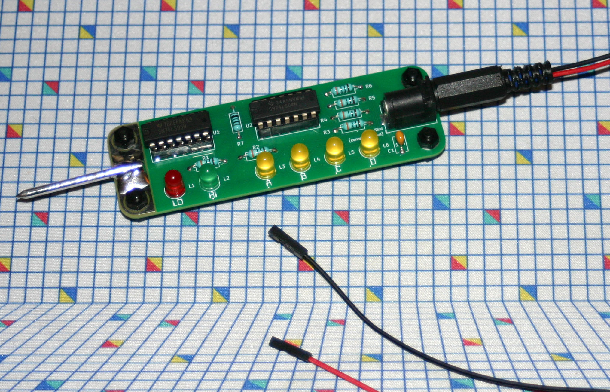
This design has a lot of functionality considering its low component count, requiring only two 7400-series ICs, seven resistors and six LEDs.
In theory, this probe should work with signals as fast as ~65MHz, the maximum speed of 74LS logic. If nothing else limits the probe's speed, you could raise this maximum to ~90MHz by using 74ALS chips instead. (Again, this is theoretical - the highest speed I've used it at so far is 14MHz.)
Being a TTL design, this probe will only work with 5V logic signals (and a 5V power source!). Since it's a very simple circuit, it may be possible to substitute the 74LS ICs for 74HC. (HC = Hi-speed CMOS, 2-6V supply voltage range)
The best method I've found is to buy a set of copper nails (look for the thinnest nails possible), coating one in solder to prevent oxidation, cutting off the head of the nail and soldering it onto the large solder pad at the end of the PCB, as seen in the above photo. I recommend using a lot of flux on the nail and solder pad. (Remember to clean it off afterwards!) This is the method I used for the probe seen in the photo at the top of the page.
Preparing and attaching the nail should be the first thing you do, since it's the most difficult thing to solder to the PCB.
Like most logic probes, you must connect it to the 5V voltage supply of the circuit you are testing. A standard barrel jack on the back of the probe allows for easy replacement of the power cable, as different circuits are likely to have different kinds of connection points available for connecting to VCC and GND.
The most versatile connectors to put on the end of the cable are a pair of female 2.54mm DuPont connectors. These can be connected to pin headers and IDC ribbon cable connectors.
![]() Bill of Materials
Bill of Materials
PDF document, 69.7 KB - A list of all the components you'll need to build the probe. Applicable to both revisions.
![]() Schematic
Schematic
PDF document, 172 KB - My schematic for the logic probe. Applicable to both revisions.
![]() Revision 1 PCB Gerbers
Revision 1 PCB Gerbers
ZIP archive, 81.0 KB - A more refined version of Revision 0. Untested so far, but the circuit layout is exactly the same as Revision 0.
![]() Revision 0 PCB Gerbers
Revision 0 PCB Gerbers
ZIP archive, 69.2 KB - The original, tested PCB. This is the one pictured at the top of the page.
![]() Revision 1 KiCad Files
Revision 1 KiCad Files
ZIP archive, 405 KB - Useful if you want to make modifications to the Revision 1 PCB. Made with KiCad 8.
![]() Revision 0 KiCad Files
Revision 0 KiCad Files
ZIP archive, 389 KB - Useful if you want to make modifications to the Revision 0 PCB. Made with KiCad 8.
![]() Bill of Materials
Bill of Materials
PDF document, 68.8 KB - A list of all the components you'll need to build the probe.
![]() Schematic
Schematic
PDF document, 172 KB - My schematic for the logic probe. Same as the through-hole schematic.
![]() PCB Gerbers
PCB Gerbers
ZIP archive, 57.7 KB - The PCB for the SMD logic probe.
![]() KiCad Files
KiCad Files
ZIP archive, 381 KB - Useful if you want to make modifications to the PCB. Made with KiCad 8.
Last updated on Mar 1, 2025.
This page was first uploaded on Mar 2, 2025.
visitors since Dec 26, 2025.
Background image by tile-anon.